14+ Ic 74194 Pin Diagram Robhosking Diagram
The 7404 IC, also known as the hex inverter, is comprised of six independent inverters, each capable of transforming logic high signals to logic low and vice versa. Its versatility makes it an indispensable building block for numerous applications, ranging from basic logic gates to more complex digital circuits.
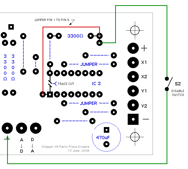
Experiment 9 DLDA Shiftreg FF Digital Logic Design And Analysis Second Year Computer
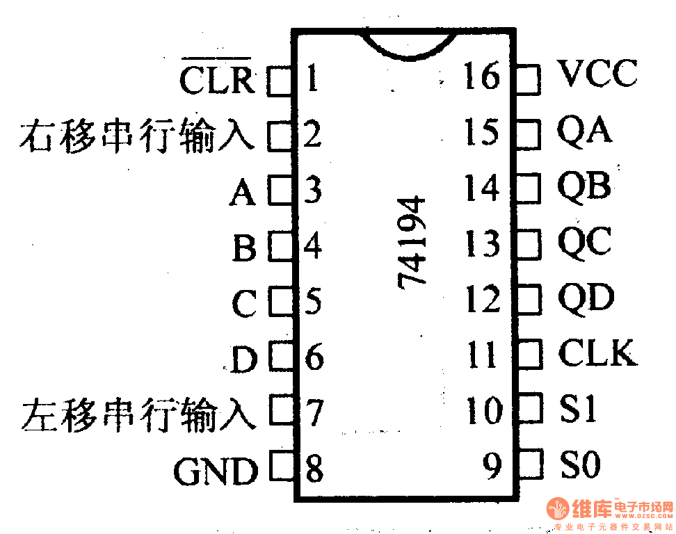
74LS194 Product details General Description This bidirectional shift register is designed to incorporate virtually all of the features a system designer may want in a shift register; they feature parallel inputs, parallel outputs, right-shift and left-shift serial inputs, operating-mode-control inputs, and a direct overriding clear line.

Universal Shift Register Parallel Input Parallel Output Register (74LS194) using Multisim
IC 7474 D-FF INTERNAL STRUCTURE PIN DIAGRAM IC 7476-INTERNAL STRUCTURE IC 7476 PIN CONFIGURATION IC 74194- INTERNAL STRUCTURE IC 74194- PIN CONFIGURATION RELATED PAPERS. Laboratory Manual EE 200 Digital Design. sravan gunturi. Download Free PDF View PDF. Local Fabrication of Digital Logic Trainer for Laboratory Demonstration.

74194 Unipolar Stepper Motor Driver
The 74HC194 is a 4-bit bidirectional universal shift register. The synchronous operation of the device is determined by the mode select inputs (S0, S1). In parallel load mode (S0 and S1 HIGH) data appearing on the D0 to D3 inputs, when S0 and S1 are HIGH, is transferred to the Q0 to Q3 outputs.
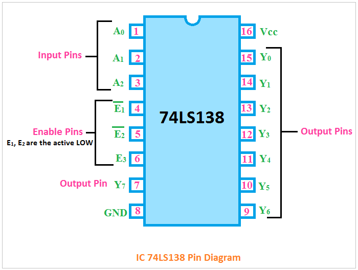
IC 74138 Pin Diagram, Truth Table, Logical Circuit, Applications ETechnoG
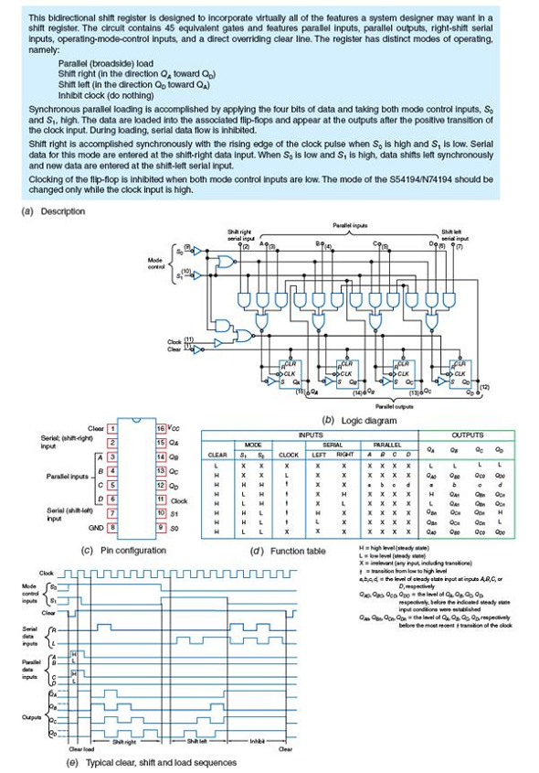
These bidirectional shift registers are designed to incorporate virtually all of the features a system designer may want in a shift register. The circuit contains 46 equivalent gates and features parallel inputs, parallel outputs, right-shift and left-shift serial inputs, operating-mode-control inputs, and a direct overriding clear line.
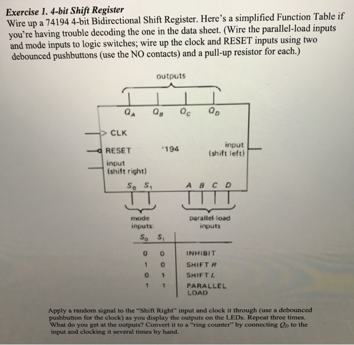
Solved Exercise 1. 4bit Shift Register Wire up a 74194
The 74LS194 bidirectional shift register is designed to incorporate virtually all of the features a system designer may want in a shift register; they feature parallel inputs, parallel outputs, right-shift and left-shift serial inputs, operating-mode-control inputs, and a direct overriding clear line. The register has four distinct modes of.
74 Series digital circuit of 74194,74LS194A 4bit twoway general shift register Digital
Description 4 BIT PIPO SHIFT REGISTER 74194 Datasheet (HTML) - STMicroelectronics 74194 Product details DESCRIPTION TheM54/74HC194 isahigh speed CMOS 4BIT PIPO SHIFT REGISTER fabricated in silicon gate C2MOS technology. It has the same high speed performance of LSTTL combined with true CMOS low power consumption.

IC 74194 Electroslab
50 3.6K views 2 years ago Digital Logic Design Experiments In this video we will learn about all modes and operations of Universal Shift Register and Implement it using 74194 IC.more.more

Seymour Duncan Little 59 Wiring Diagram Circuit Diagram
74LS194. 74LS194. 4-Bit Bidirectional Universal Shift Register. General Description Features. This bidirectional shift register is designed to incorporate n Parallel inputs and outputs virtually all of the features a system designer may want in a n Four operating modes: shift register; they feature parallel inputs, parallel outputs, Synchronous.

IC741 Pin Diagram Pin Diagram of IC741Pin configuration of IC741 OpAmp IC741 pin Diagram
74192 ic pin diagram/ 74192 ic pin configuration. 74192 Truth Table. BCD, or Binary Coded Decimal, is a common counting sequence in which each decimal digit is represented by a 4-bit binary code. In a BCD decade counter, the counting sequence is as follows: Up-Counting Sequence: 0000 (0 in BCD) 0001 (1 in BCD) 0010 (2 in BCD) 0011 (3 in BCD.

Op Amp Pin Diagram General Wiring Diagram
TI's SN74LS194A is a Bidirectional universal shift registers. Find parameters, ordering and quality information

DLD Lab Ring Counter using IC 74194 YouTube
Design and implement pulse train generator using IC74HC194 for pulse 111001 (Use left shift) Show circuit diagram. ICs used: 74HC194 74LS04 74LS32. Design and Implement 4-bit right shift register using D-flip flop Show circuit diagram. ICs used: 74LS74. Learn to build Universal Shirt Register using 74LS194 step by step with our virtual trainer.

View 8 Bit Johnson Counter Truth Table Images Cody M. Foster
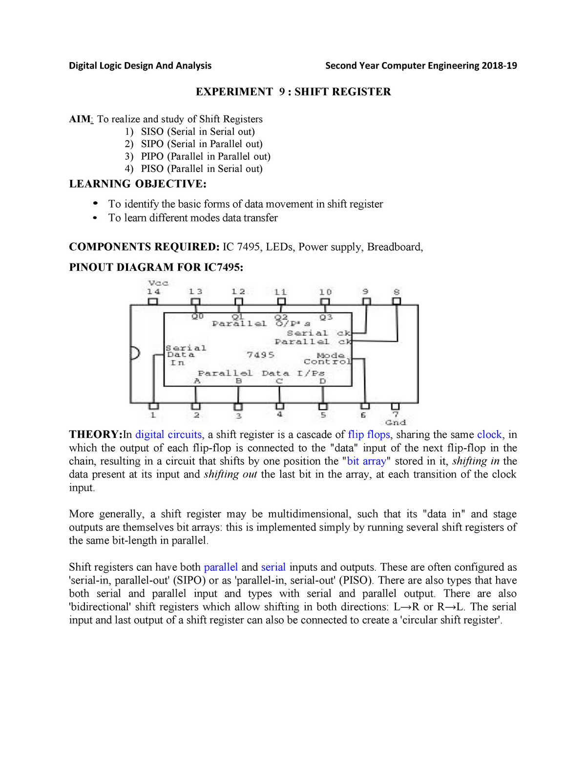
Internal Logic Diagram The logic diagram of the 74LS164 shift register IC is shown in the figure below. It internally consists of 8 flip flops, one AND and two Not gates. Truth Table The Truth Table for working of IC is shown in the figure below. Equivalent ICs: 74LS165, 74LS166, 74LS170, 74LS295 74LS164 Shift Register Working
Buy Online 74LS194 4bit Bidirectional Shift Register IC (74194 IC) DIP16 Package
TI's CD74HCT194 is a High Speed CMOS Logic 4-Bit Bidirectional Universal Shift Register. Find parameters, ordering and quality information
Solved Refer to Fig. 96. The 74194 IC is triggered on the_______...
In figure 7.4, a serial load shift right register has been demonstrated, which is of 74194 - IC type. As this 74194 - IC register is a universal shift register, therefore when it is used as a shift right register, its mode control (S 0, S 1) should be on shift right position according to the picture (i.e. S 0 must be on 1 whereas S 1 on 0).
7475 pin diagram HasanChelsay
Notes. S 0 and S 1 are low; hold (do nothing) S 0 low and S 1 high; shift left. S 0 high and S 1 low; shift right. S 0 and S 1 high; parallel load. Note: Data is maintained by an independent source and accuracy is not guaranteed. Check with the manufacturer's datasheet for up-to-date information.